Faculty of Electrical Engineering introduced Nanolaboratory, a laboratory for nanoelectric technologies for 40 million CZK
The new laboratory will satisfy the demand of Czech companies for experts in the design and implementation of semiconductor chips.
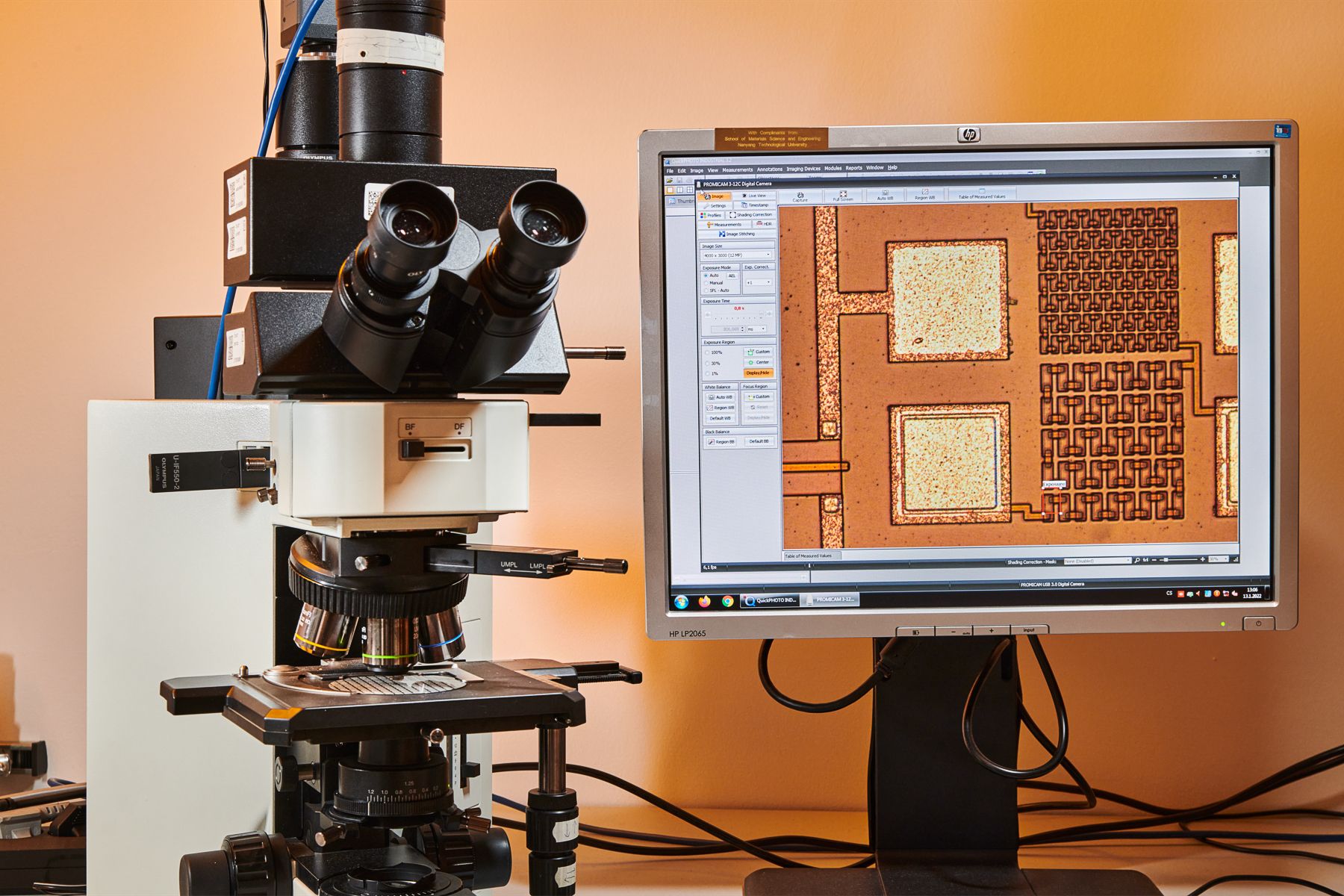
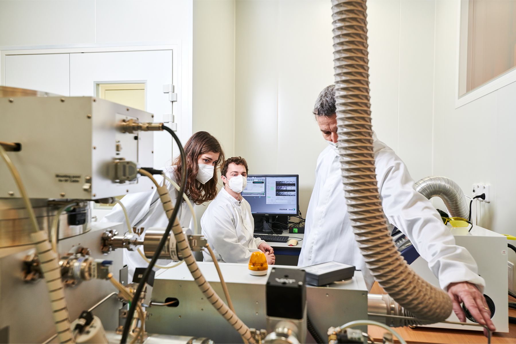
The Faculty of Electrical Engineering of CTU (FEL) inaugurated Nanolaboratory, a laboratory for research and teaching of nanoelectric technologies. The new laboratory, which was created with an investment of 40 million CZK, combines several unique technologies into one unit. Its capabilities will benefit both researchers from the Department of Microelectronics and students, who will gain hands-on experience with high-tech devices used in the semiconductor industry.
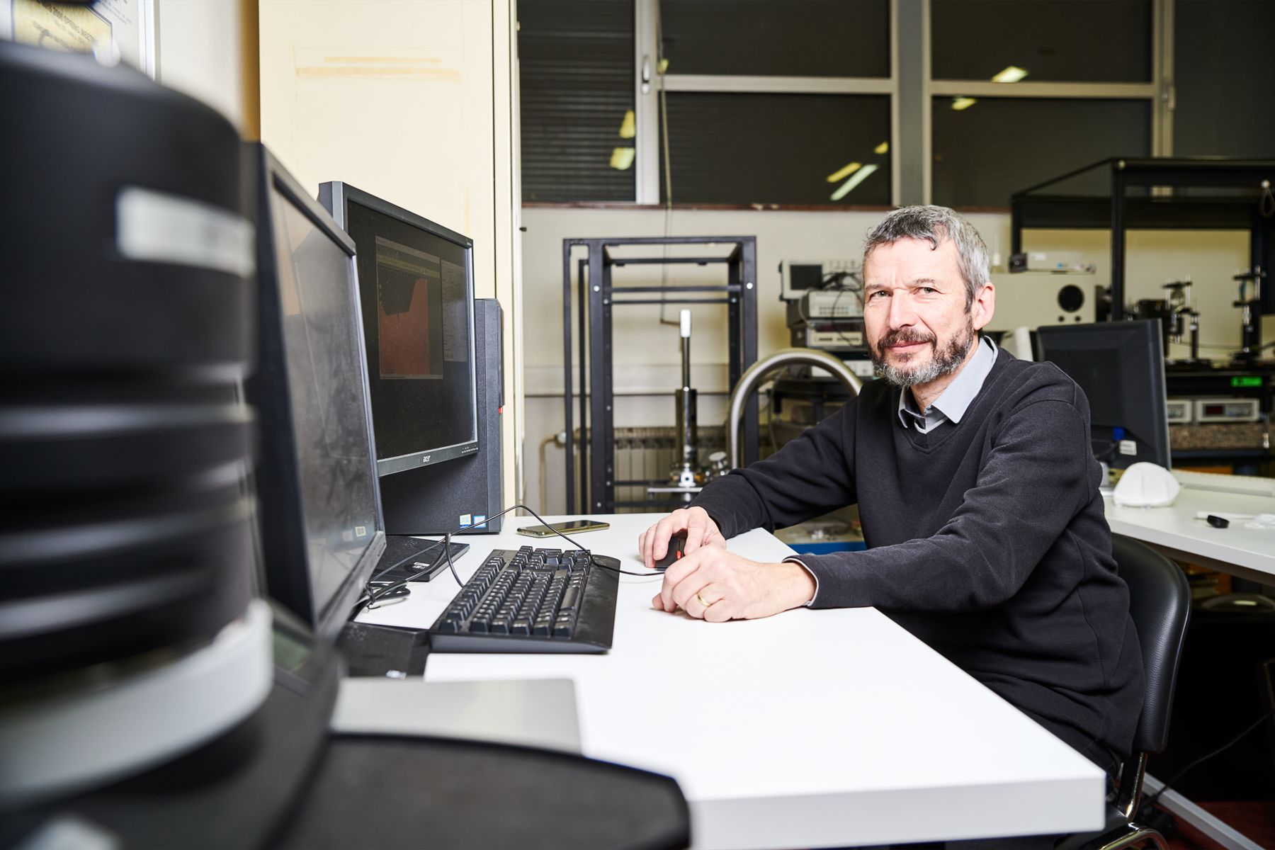
All the projects that have been started in Nanolaboratory last year during its test run are mainly carried out by PhD students, but also by Bachelor's and Master's students. "The laboratory is currently used by five PhD students, several postdoctoral fellows, and four research and teaching staff," says Jan Voves, head of the new laboratory and associate professor at the Department of Microelectronics.
Nanolaboratory will thus significantly contribute to meeting the demand of Czech companies for highly specialized experts who will design semiconductors, including microchips, the lack of which significantly affects the global markets. Companies in the field of semiconductor manufacturing need not only technologists, but also designers, whose knowledge and competences are being developed by the new laboratory at the Department of Microelectronics. Graduates will be in great demand by small and large companies involved in the production of microchips, optical components and electronic components.
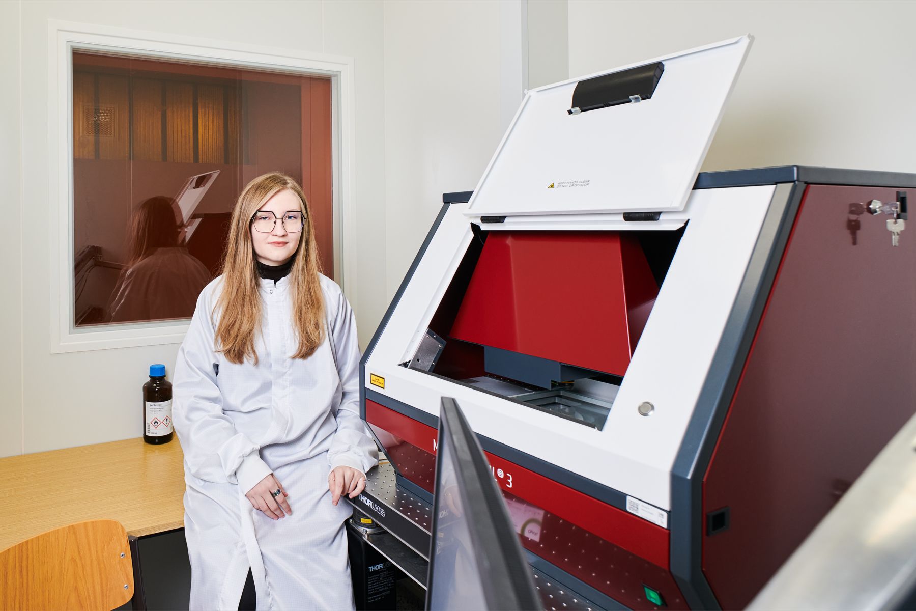
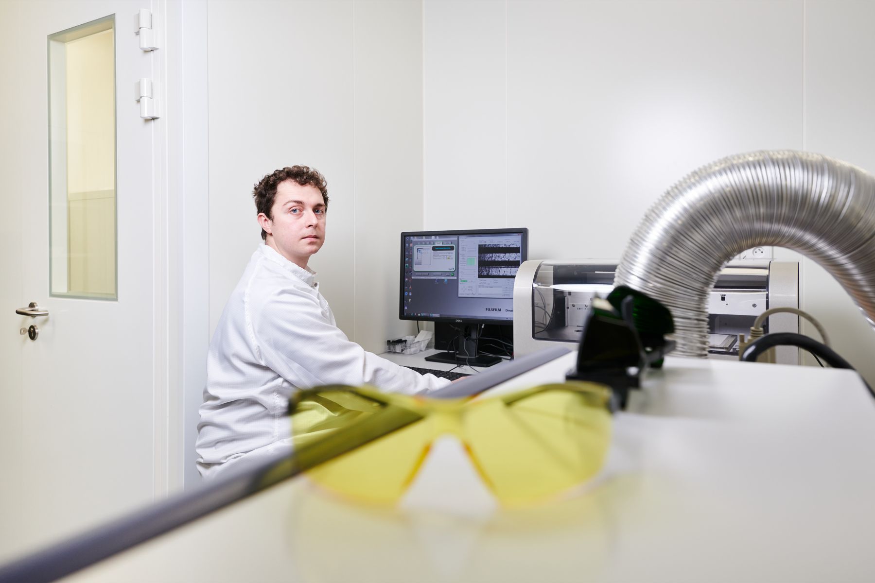
One of the students who is implementing her project in Nanolaboratory is Bc. Karolína Veselá. As part of her bachelor thesis she participated in the operationalization of thin film deposition technology. "The Atomic Layer Deposition (ALD) device is able to grow a new layer of material on the sample, even in the order of single molecules, thanks to successive chemical reactions in the reactor. Several test growths of thin oxide layers have been successful," explains a first-year student in the Master's programme in Electronics and Communications. Karolína Veselá plans to use the technology in her master's thesis and eventually also in her doctoral thesis, most recently in cooperation with the Institute of Physics of the CAS, where they have a similar MBE technology.
Where Nanolaboratory will contribute to new knowledge: cancer cell research, solar cells or space research
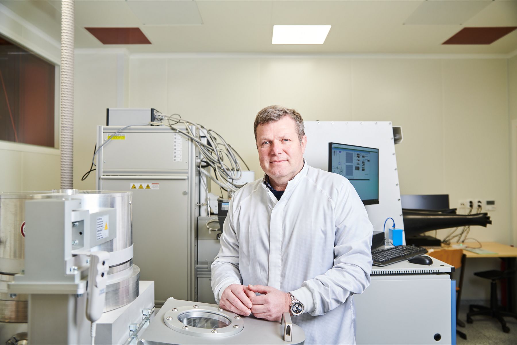
However, the spectrum of fields that Nanolaboratory will contribute to is much broader than just chips. "Nanolaboratory will increase our understanding of the new technologies and challenges facing our society. We are preparing to collaborate on the development of anti-reflective layers for solar cells in collaboration with a laboratory that operates within our faculty. This will also help us in our projects with diamond electronics, which are highly durable. Another area of application is space technology, in which both the public and private sectors are involved," says Prof. Pavel Hazdra, Head of the Department of Microelectronics at FEL CTU, outlining the potential for further interdisciplinary research and the breadth of applications that researchers from his department will be able to develop thanks to the Nanolaboratory.
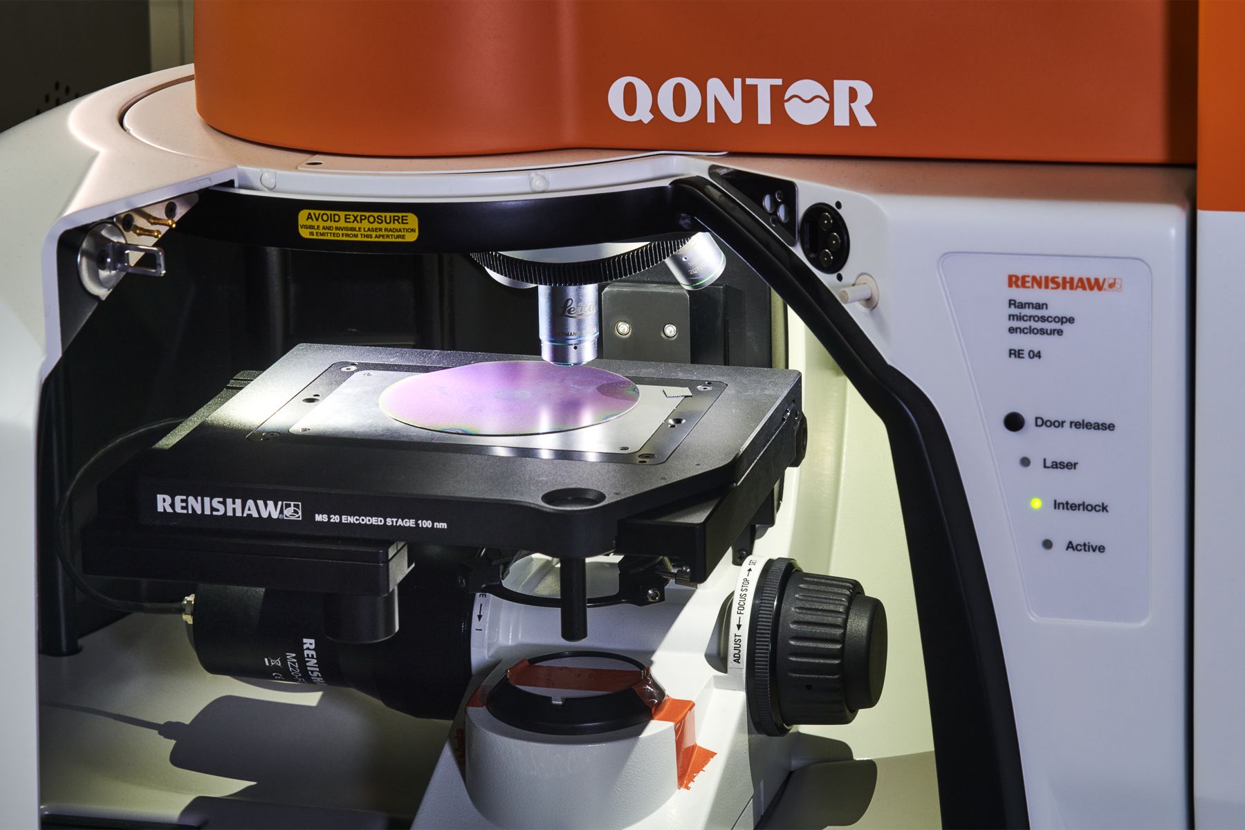
The team of doc. Jan Vovsa has already started cooperation with National Taiwan University of Science and Technology (NTUST), which performs non-destructive measurements of biological substances using Raman spectroscopy (Surface Enhanced Raman Spectroscopy). "This technology has the ability to amplify the signal with the help of surface modification, and in the project we are using ALD technology to create dielectric layers in Nanolaboratory to enable better detection of biological substances. Although this is still basic research, there is already an overlap with a specific application in the medical field; with the help of this spectroscopy, it is possible to detect cancer cells," doc. Vovsa explains the research with the University of Taiwan already carried out.
Nanolaboratory as an outcome of a long tradition in microelectronics research at FEL CTU
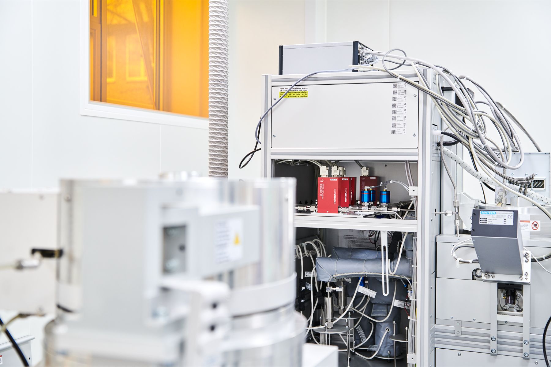
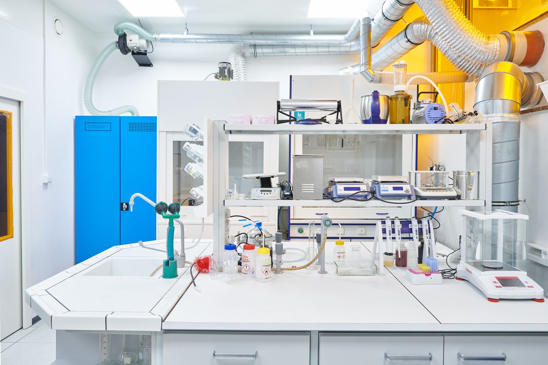
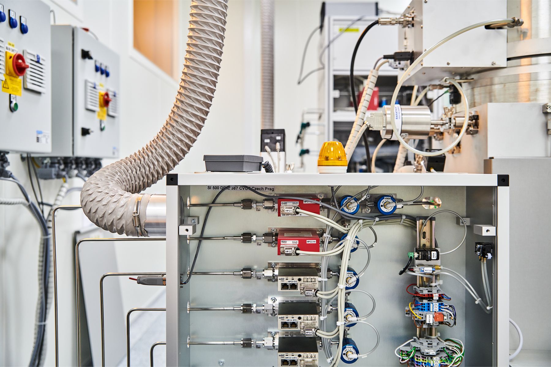
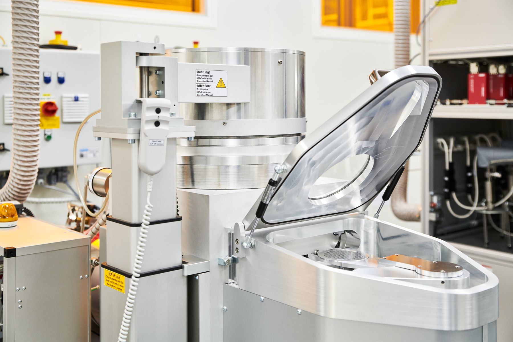
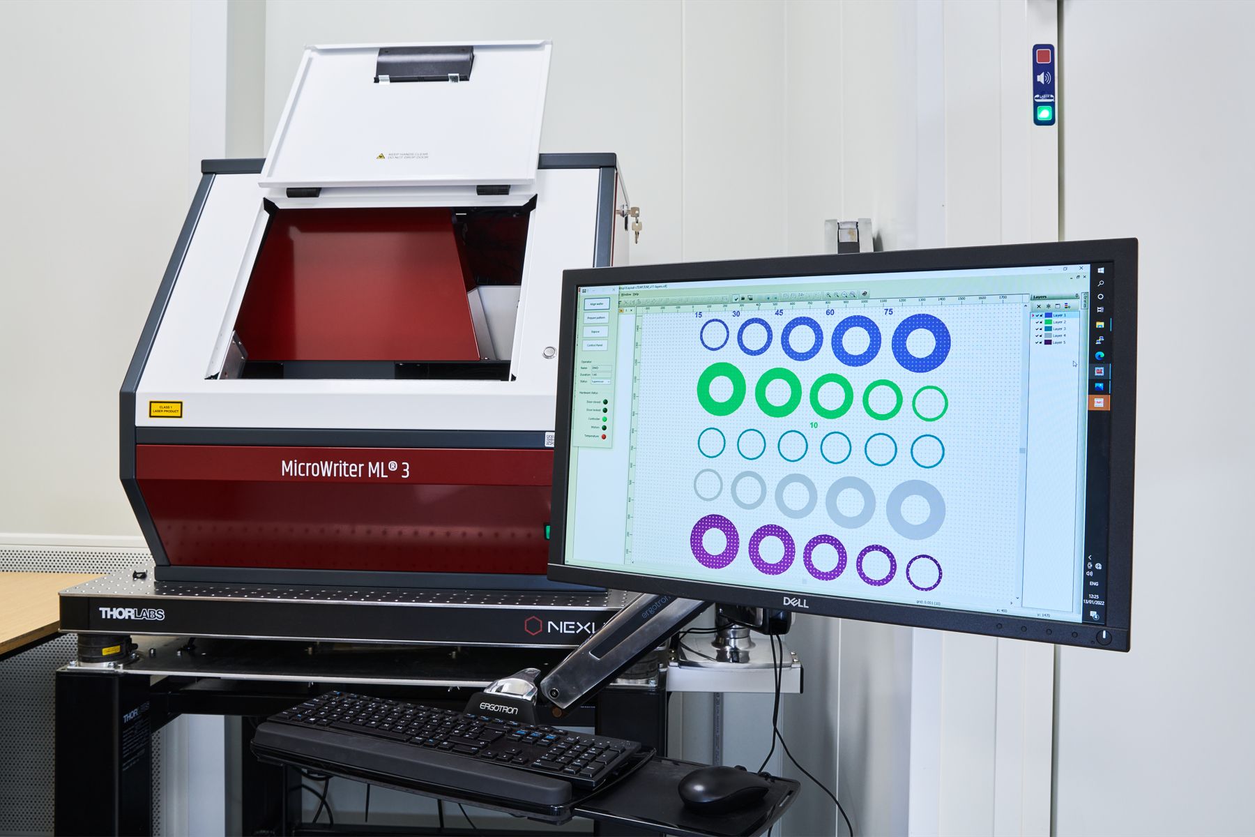
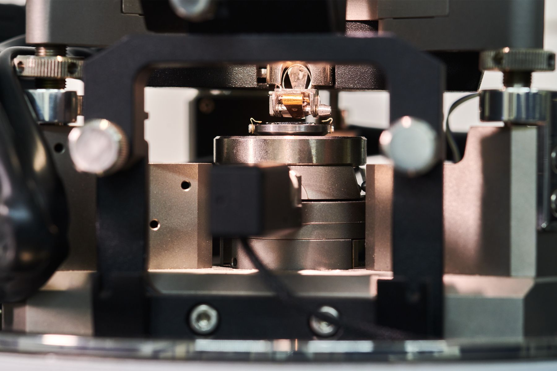
The Nanolaboratory is equipped with unique technologies in the areas of maskless optical lithography, atomic layer deposition (ALD) and deep etching with reactive plasma, which form a complete system located in a high clarity area. "Some of the instruments have not been seen in the country before, such as the latest model of the ML3 direct-write optical lithography machine. The ALD technology in our laboratory has the advantage of very gentle sample insertion using a load-lock transition chamber located in a nitrogen atmosphere and also in monitoring growth using optical ellipsometry, allowing growth to stop when a certain number of atomic monolayers are reached," says Prof. Pavel Hazdra. It is on the growth of the dielectric layers of the ALD technology that the undergraduates will become familiar with the instruments, so that they can then go on to create their own structures later in their master's studies.
The Nanolaboratory was established in connection with the Laboratory of Nanoelectronics, equipped with an AFM microscope, a material printer and characterization methods between 2012 and 2015 with support from the Ministry of Education and Science. Thanks to the projects Research Infrastructure for Doctoral Programmes at CTU FEL and the Centre for Advanced Applied Sciences for the Development of Doctoral Studies and CAAS, it was possible to gradually renovate the laboratory between 2019 and 2021 to meet the requirements for clean rooms and to equip it with costly technological equipment. Research in microelectronics at FEL CTU, however, follows a longer tradition that dates back to the late 1960s and early 1970s. The state of the art and technology at that time is captured in a popularisation document from 1980 entitled Microelectronics Implementation Project.


Photo, courtesy of: Petr Neugebauer, Faculty of Electrical Engineering CTU